")
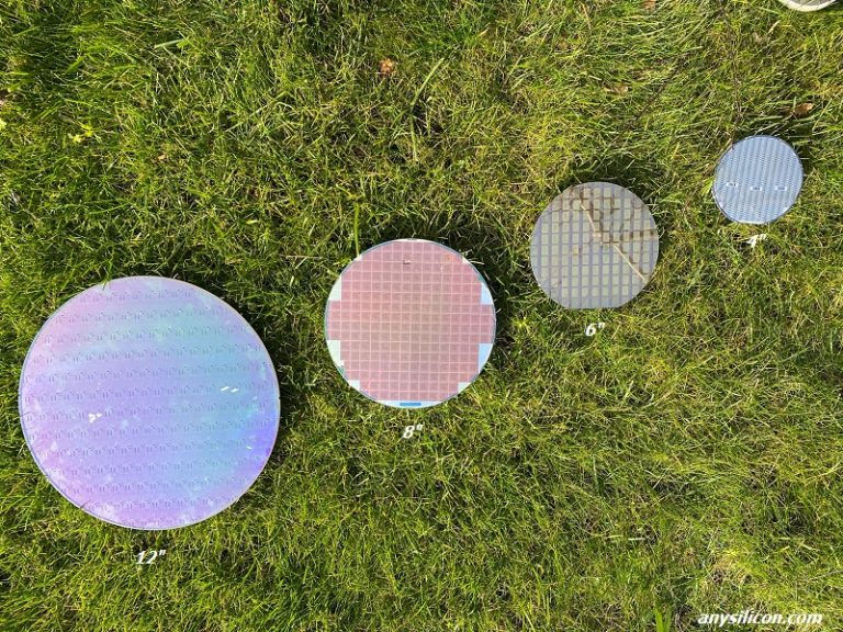
In the 1980s, Bell Laboratories had its own on-site integrated circuit fabrication facility, used both to produce circuits for use in its projects and in research related to semiconductor fabrication processes. The device geometries of the era were sufficiently large and forgiving that the standards of clean room operation were far more relaxed than in present-day facilities, and the 150 mm wafers of the era have now been supplanted by 300 mm wafers (four times the surface area) in leading chip manufacturing plants. Here is the evolution of wafer size from the 1980s to the present.