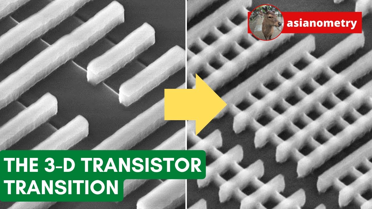
As transistor size shrank with the scaling of integrated circuits toward 25 nanometres, inherent leakage through the silicon substrate caused the MOSFET transistors almost universally used in these circuits to malfunction. Seeing this limit approach, in 1997 DARPA contracted with a lab at the University of California Berkeley to research device geometries which could escape this limitation. By 2001 the project has demonstrated a 15 nanometre transistor using a three-dimensional structure called “FinFET”, and the next year built a 10 nanometre device.
In the 2000s, the major semiconductor foundries including Taiwan Semiconductor Manufacturing Company (TSMC), Samsung, and Intel developed commercial processes to manufacture FinFET circuits and brought products to market in the 2010s. Today, most circuits at the 14, 10, and 7 nanometre scales use FinFET gates.
The end of the video explores the limits on FinFET scaling to smaller geometries, possible work-arounds, and speculates on whether the fabrication cost will price the technology out of the market.
Note that while individual transistors have a three-dimensional structure, the overall layout of integrated circuits remains planar. The industry has only taken baby steps toward true three-dimensional integrated circuits through means such as stacking “chiplet” dice atop one another with broad-based chip-to-chip interconnections.
