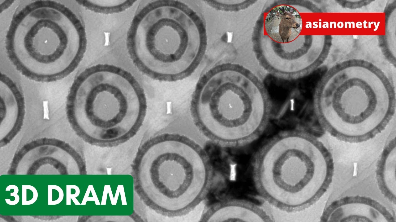
As demand for ever greater capacity semiconductor memory chips grew, first designs were simplified to use just a single transistor and capacitor storage element per bit, and then device geometries were scaled smaller and smaller, allowing more bits to be packed onto a chip (while simultaneously reducing power consumption). But eventually this scaling began to run into the limitations of those pesky laws of physics—in particular, when the size of the capacitor that stores electrons whose presence or absence distinguishes a “1” from a “0” bit shrinks beyond a certain size, it can’t hold sufficient electrons to reliably separate the two bit values in the presence of thermal and electrical noise, imperfections in fabrication, and quantum mechanical effects. Stop shrinking device geometries—never! Clever chip designers figured out how to escape into the third dimension, using tricks such as stacked or trench capacitor geometries to increase the size of the electron storage per bit without using space in the planar memory array. This further increased the complexity of fabricating these structures, but the increased capacity and the market’s voracious demand for memory justified the investment in learning how to produce them in volume. Further increases in density were achieved by adopting exotic high dielectric constant materials for capacitors, such as tantalum pentoxide, hafnium silicate, and barium strontium titanate.
2 Likes
