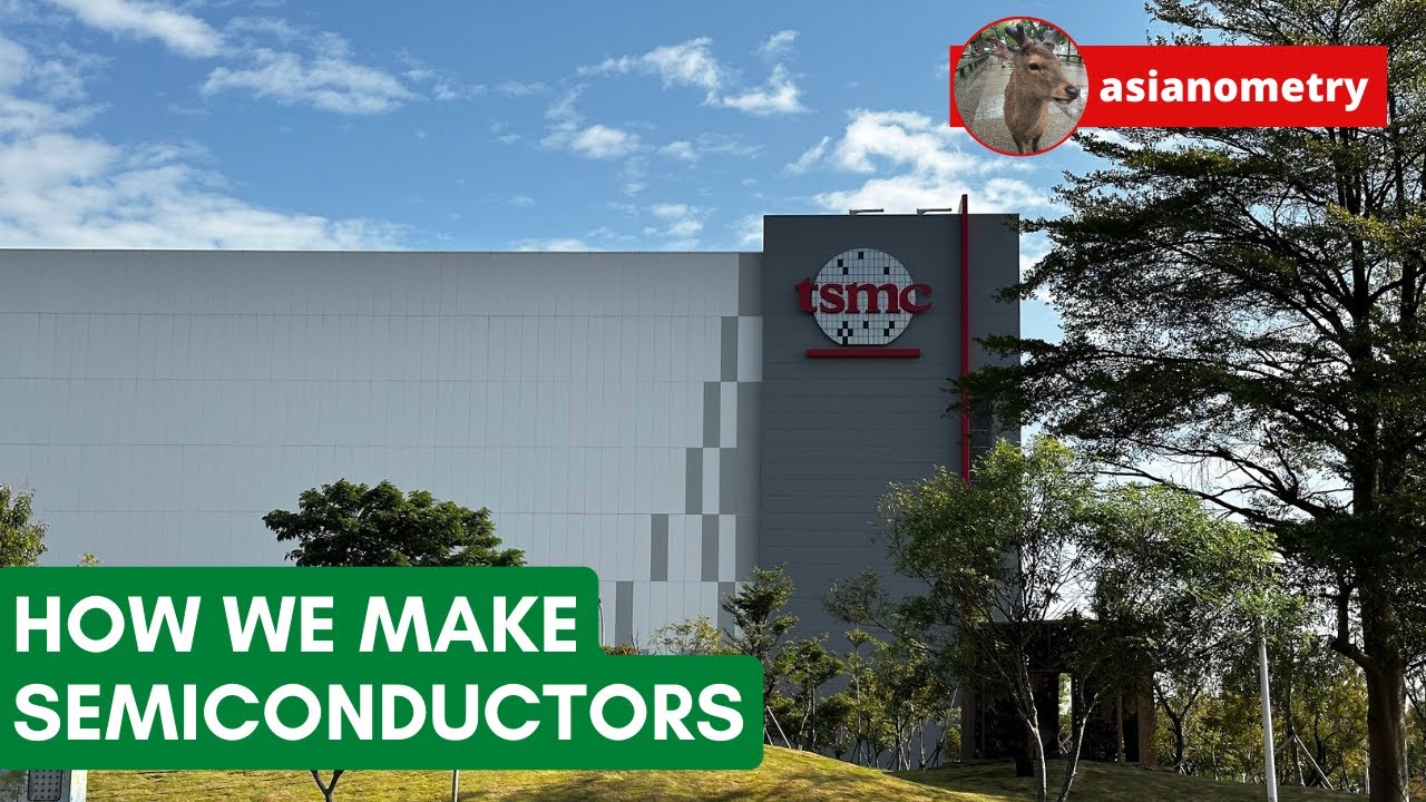
There is a lot more to making a wafer full of semiconductor chips than photolithography, and many more vendors in the supply chain than ASML. Here is a look at the entire fabrication process, from silicon boule to ready-to-package chips. Understanding these steps helps explain why these facilities occupy 950,000 square metres of floor space, cost US$ 20 billion to build and equip, and take years to come on line. Glib politicians who speak of achieving “semiconductor autonomy” in a short period of time do not appear to be aware of these details.
5 Likes
