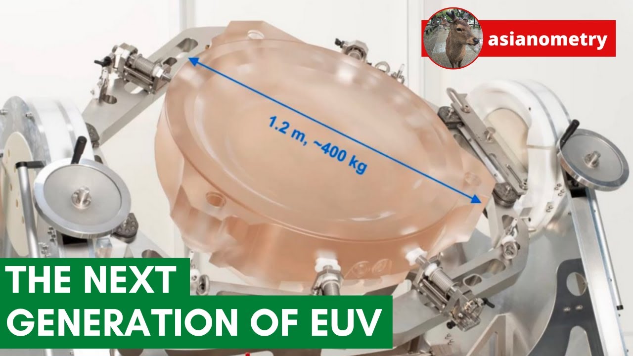
In order to further reduce the size of features on integrated circuits and thus increase transistor counts, tricks such as multiple patterning will be required. These run the risk of reducing throughput in the photolithography process, driving up costs. One way to avoid this is to increase the numerical aperture (NA) of the optical system that exposes the photoresist on the silicon wafer. This, in turn, requires a whole bag of dirty tricks and over-the-top optics, with the next generation photolithography machines which will use it expected to be around the size of a school bus and cost around US$ 300 million a pop. First customer deliveries by ASML are expected in late 2022.
3 Likes
