
Photolithography, the fundamental technology used in almost all integrated circuit manufacturing, is pretty simple in concept: you make a mask for the pattern you wish to lay down on the chip, apply a photo-sensitive resist uniformly to the chip, expose it to light through the mask, wash away the portion the mask indicates should be processed in the next step, and then etch, deposit material, or implant material on the non-masked regions. The details of this are exquisitely complicated and require great precision, but the idea of manufacturing complicated devices by what amounts to printing pictures of them is the simple concept that underlies the greatest revolution in mass production in human history.
Since their inception in the late 1950s, integrated circuits have simultaneously shrunk the size of the devices that compose them while increasing their density and complexity. I remember, in the late 1960s, reading forecasts that this process would have to come to an end when the device geometries shrank to smaller than the wavelength of light used to print the mask onto the chip substrate. Well, that didn’t take into account the cleverness of engineers, physicists, optical designers, and creators of computer-aided design tools engaged in a global competition to produce the fastest, least expensive, and most complex and energy efficient circuits in a market which was growing exponentially in size.
If you think in terms of geometrical optics, it’s completely impossible to create a sharp image with features smaller than the wavelength of light you’re using to produce it. This is why, for example, there is an absolute limit on the smallest object you can observe through a visible light microscope—to see smaller things, you need to use something like an electron microscope, which images with a far smaller wavelength. But geometrical optics considers light as composed to infinitely small rays that may be absorbed, reflected, and bent, but do not exhibit the properties due to their wave nature such as diffraction and interference. As light interacts with small features on the order of its wavelength, these phenomena increasingly dominate, and shining light through a mask with features comparable to its wavelength will produce an image that looks nothing like the pattern on the mask.
But, since light propagation is time symmetric, if you ran the light the other way, wouldn’t you get back the pattern on the mask? Well, in principle, but of course there are nasty details to be dealt with. If you could solve them, though, couldn’t you then compute the pattern on a mask which, after all the messy diffraction and interference occurred, actually printed the pattern you wanted on the chip? The mask would look nothing like the pattern on the chip, but it would make that pattern when light shone through it.
This was one of those things that were possible in principle, but required such a hideously large amount of computation that it was long considered infeasible. Over the years, chip designers learned tricks to eke more resolution out of light waves, but eventually this hocus-pocus was approaching the limit. Here is the evolution of masks to make simple horizontal and vertical traces over the years.
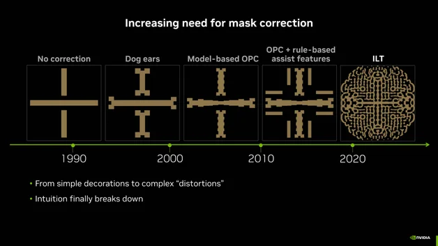
That screwball pattern at the right is the result of “Inverse Lithographic Technology” (ILT) or, as you might say, “Beating light into submission with a computer”. When you shine light through that crazy ILT mask, what you get on the chip are the lines at the very left.
The computation required to do this is daunting, especially when you consider that leading-edge chips can have billions of transistors, passive components, and interconnects, all of which must be perfect or the chip is junk. In March 2023, Nvidia, known for its graphics processing units (GPUs) and artificial intelligence accelerators, announced a new set of algorithms, collectively called cuLitho, which they claim speed up the computations of inverse lithography by a factor of forty, making it practical to deploy widely in chip design and mask making. Here is an IEEE Spectrum article about the announcement.
Nvidia claims that using cuLitho, a cluster of 500 Nvidia DGX H100 GPUs can compute masks using inverse lithography faster than an array of 40,000 of the fastest general-purpose processors available today, producing three to five times as many masks a day.
Taiwan Semiconductor Manufacturing Company (TSMC) is said to be qualifying the cuLitho process for production use this year.