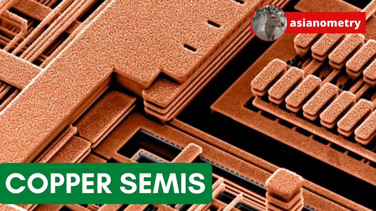
As semiconductor device geometries shrank to achieve greater complexity, faster speed, and lower power due to the Dennard scaling theorem, the physical properties of materials began to limit the ability to further reduce scale. In particular, aluminium, which had been used for integrated circuit interconnects (intra-chip “wiring”) from their early days, had electrical resistance sufficiently high that shrinking beyond a certain point would slow the operation of a chip due to the RC (resistance-capacitance) time constant of the interconnect. This was most unfortunate, since aluminium is an almost ideal material in many ways: inexpensive, easy to deposit on chips by various methods, and well-behaved in conjunction with silicon substrates. But unless something that performed better electrically was found, chip performance would hit a hard wall around the year 2000. Copper had conductivity almost 60% better than aluminium, but the difficulties in integrating it into the semiconductor fabrication process were formidable: the techniques that worked so well with aluminium couldn’t handle copper and, once applied to a chip, copper would tend to migrate into silicon structures, destroying devices and creating short circuits. When, in the late 1990s, IBM reported success in fabricating integrated circuits with copper interconnects, rival companies scarcely believed it, since the difficulties were so formidable, but then had to scramble to catch up. It was in this process that Taiwan Semiconductor Manufacturing Company (TSMC) began to pull ahead and become the world leader in semiconductor fabrication it is today.
3 Likes
