With device geometries on semiconductor chips continuing to shrink in order to pack ever more transistors onto a chip, semiconductor manufacturers reached a point where the device features they needed to make were smaller than the wavelength of visible light, previously used to print structures on chips through the process of photolithography. High-end chip manufacturers such as Taiwan Semiconductor (TSMC), Samsung, and Intel have migrated their cutting edge fabrication to extreme ultraviolet photolithography (EUV), using a wavelength of 13.5 nanometres, a part of the electromagnetic spectrum previously called “soft X-rays” before being renamed to something less scary. (By comparison, visible light is in the range from 380 [violet] to 750 [red] nanometres.)
EUV is a technology which not only allows building things never imagined during the golden age of science fiction, it is made up of parts that, had Doc Smith dropped them into one of his Skylark novels, would have been considered techno-confabulation (“400,000° Celsius laser-driven tin plasma light source”).
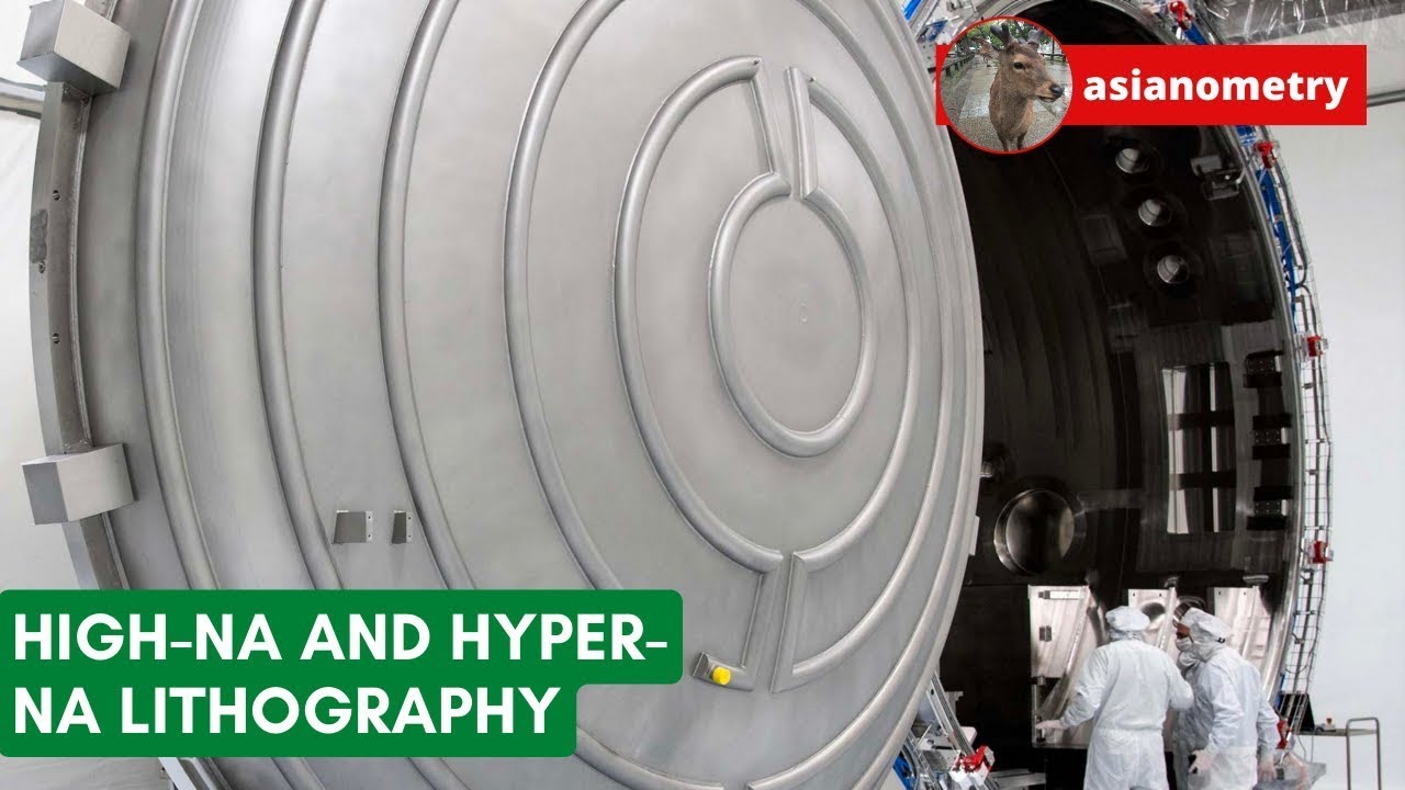
But, as those who wish to survive in the semiconductor business must constantly ask, “What’s next?” As node sizes scale below the next major milestone of 3 nanometres, the sole survivor in the high-end photolithography market, Netherlands’ ASML (formerly Advanced Semiconductor Materials Lithography before, like all big companies, it decided a meaningless name was more appropriate) has decided the next milestone will be achieved by increasing what is called the “numerical aperture” of its photolithography machines. Numerical aperture (NA) is a dimensionless quantity that measures the amount of light an optical system can deliver to its target (similar to an f-stop in visible light photography). Present-day EUV machines from ASML have a NA of 0.33, which allows a resolution of 13 nanometres (note that the optical resolution of the photolithography machine, the feature size on the chip, and the “node size” of the process are all different things, with the latter having more to do with the marketing department than engineering or manufacturing). The next generation high numerical aperture (high-NA) EUV machines under development by ASML aim to increase NA to 0.55, initially allowing 8 nanometre resolution, with scaling to as small as 3 nanometres in the future. This requires hardware even more science-fictioney than existing EUV, but also revision of the entire fabrication process. Masks (the master pattern printed on the chips), photoresists (exposed by the lithography process), and even the silicon wafers and positioning equipment (that must have extraordinary flatness and precision to cope with the minuscule depth of field at such resolutions) must adapt. Here is an overview from Semiconductor Engineering, “Gearing Up For High-NA EUV”.
None of this comes cheaply. High-NA EUV lithography machines are estimated to cost around US$ 320 million each, around twice the cost of existing EUV machines, with higher costs all along the processing chain.
And beyond? ASML expect to deliver the first high-NA (0.55 NA) machine for prototyping before the end of 2023, with production shipments starting in 2025. Looking further out, forecasters envision “hyper-NA” technology, increasing numerical aperture as high as 0.75, to be introduced around 2035. ASML Chief Technical Officer Martin van den Brink isn’t so sure that’s going to happen—in a September 2022 interview, he said:
We’re researching it, but that doesn’t mean it will make it into production. For years, I’ve been suspecting that high-NA will be the last NA, and this belief hasn’t changed.
For ‘standard’ EUV, the NA is 0.33, for high-NA, it’s 0.55 and for hyper-NA, it would be “above 0.7, maybe 0.75. Theoretically, it can be done. Technologically, it can be done. But how much room is left in the market for even larger lenses? Could we even sell those systems? I was paranoid about high-NA and I’m even more paranoid about hyper-NA. If the cost of hyper-NA grows as fast as we’ve seen with high-NA, it will pretty much be economically unfeasible. Although, in itself, that’s also a technological issue. And that’s what we’re looking into.
⋮
We were going to make sure that high-NA would happen. For hyper-NA, we’re accepting that there may be an insurmountable cost constraint, not in the least because transistor shrink is slowing down. Thanks to system integration, it will still be worthwhile to keep developing new chip generations – that’s the good news. But at this point, the question has become very real: which chip structures are too small to manufacture economically?
We shall see. Perhaps by then our artificial intelligence overlords will figure out how to do it and command us to make it so.
