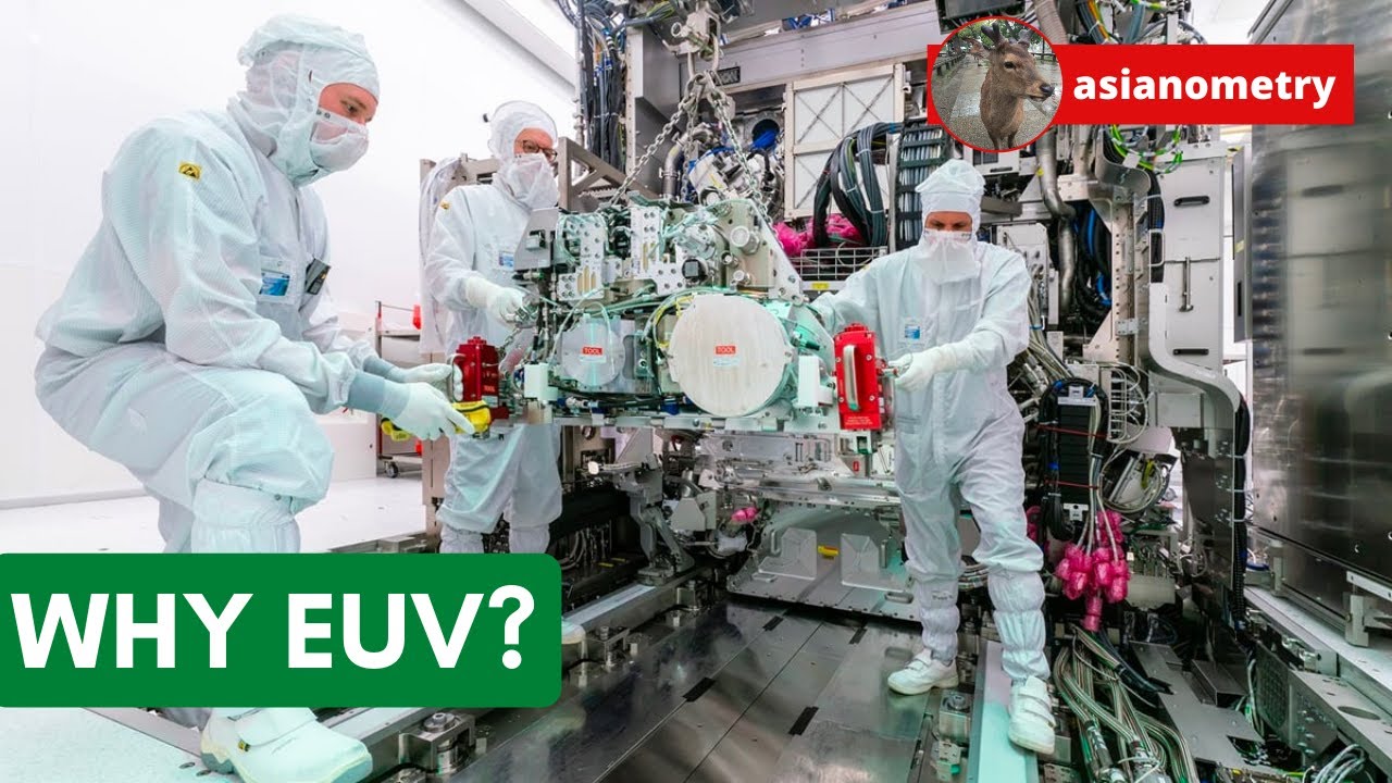
With the scaling of semiconductor component geometries first to smaller than the wavelength of visible light, then below the size of ultraviolet light, the semiconductor industry was faced with a crucial decision: which technology would permit continuing to fit more transistors on a chip while preserving speed of manufacturing and yield of functional chips per wafer to remain cost-competitive with earlier generation processes?
Whatever technology was chosen would take on the order of a decade to develop and deploy and require investment of tens of billions of dollars in process equipment by manufacturers employing the new technology. Among the competing candidate processes, extreme ultraviolet lithography (EUV) (also called “soft X-ray lithography” before that name fell out of favour because it sounded too scary) won out and is now used by all industry leading semiconductor manufacturers. How and why did it win, and what may be next when the its limits are reached?
For the extreme technology involved in just generating extreme ultraviolet light, see the post from 2021-12-30, “Extreme Ultraviolet Light Source”.
