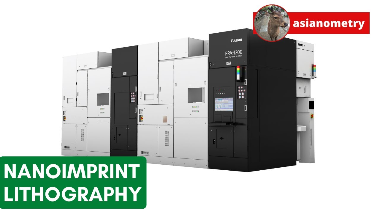
Photolithography has long been the leading technology for production of high-density integrated circuits, and its latest incarnation, extreme ultraviolet (EUV) photolithography, is used today for producing state of the art chips (see “How the Semiconductor Industry Chose Extreme Ultraviolet Lithography”, posted here on 2023-06-16). But it isn’t the only way to transfer tiny patterns to chip substrates. A competitive technology, developed since the mid-1990s and commercialised by Canon in Japan, “nanoimprint lithography”, literally stamps tiny patterns onto a thermoplastic resist applied to the chip with a mould, often itself fabricated by other forms of lithography. Wikipedia notes in the article linked above:
A key benefit of nanoimprint lithography is its sheer simplicity. The single greatest cost associated with chip fabrication is the optical lithography tool used to print the circuit patterns. Optical lithography requires high powered excimer lasers and immense stacks of precision ground lens elements to achieve nanometer scale resolution. There is no need for complex optics or high-energy radiation sources with a nanoimprint tool. There is no need for finely tailored photoresists designed for both resolution and sensitivity at a given wavelength. The simplified requirements of the technology lead to its low cost.
There are, of course, compensating drawbacks. At present, fabrication of structures smaller than 10 nanometres has not been demonstrated, and wear on the mould (or template) may limit its service life. But as photolithography confronts ever more difficult barriers due to the inescapable limits of electromagnetic radiation, literally stamping out chips may provide an alternative.
